- 您现在的位置:买卖IC网 > Sheet目录3890 > PIC16C765T-I/L (Microchip Technology)IC MCU OTP 8KX14 USB 44PLCC
2000 Microchip Technology Inc.
Preliminary
DS41124C-page 141
PIC16C745/765
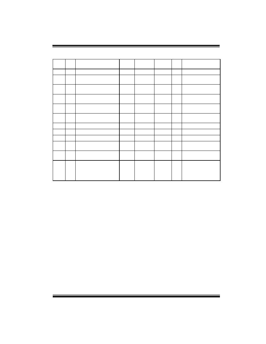
TABLE 16-10: A/D CONVERTER CHARACTERISTICS: PIC16C745/765 (INDUSTRIAL)
Param
No.
Sym
Characteristic
Min
Typ
Max
Units
Conditions
A01
NR
Resolution
——
8 bits
bit
A02
EABS
Total Absolute error
——
< ± 1
LSb
VREF = VDD = 5.12V,
VSS
≤ VAIN ≤ VREF
A03
EIL
Integral linearity error
——
< ± 1
LSb
VREF = VDD = 5.12V,
VSS
≤ VAIN ≤ VREF
A04
EDL
Differential linearity error
——
< ± 1
LSb
VREF = VDD = 5.12V,
VSS
≤ VAIN ≤ VREF
A05
EFS
Full scale error
——
< ± 1
LSb
VREF = VDD = 5.12V,
VSS
≤ VAIN ≤ VREF
A06
EOFF
Offset error
——
< ± 1
LSb
VREF = VDD = 5.12V,
VSS
≤ VAIN ≤ VREF
A10
—
Monotonicity (Note 3)
—
warranteed
——
VSS
≤ VAIN ≤ VREF
A20
VREF
Reference voltage
2.5V
—
VDD + 0.3
V
A25
VAIN
Analog input voltage
VSS - 0.3
—
VREF + 0.3
V
A30
ZAIN
Recommended impedance of
analog voltage source
——
10.0
k
A40
IAD
A/D conversion current (VDD)
—
180
—
A
Average current consump-
tion when A/D is on (Note 1)
A50
IREF
VREF input current (Note 2)
10
—
1000
10
A
During VAIN acquisition.
Based on differential of
VHOLD to VAIN to charge
During A/D Conversion cycle
*
These parameters are characterized but not tested.
Data in “Typ” column is at 5V, 25
°C unless otherwise stated. These parameters are for design guidance only and are not
tested.
Note 1:
When A/D is off, it will not consume any current other than minor leakage current. The power-down current spec includes
any such leakage from the A/D module.
2:
VREF current is from the RA3 pin or the VDD pin, whichever is selected as a reference input.
3:
The A/D conversion result never decreases with an increase in the input voltage and has no missing codes.
745cov.book Page 141 Wednesday, August 2, 2000 8:24 AM
发布紧急采购,3分钟左右您将得到回复。
相关PDF资料
PIC18C442T-E/L
IC MCU OTP 8KX16 A/D 44PLCC
PIC16C621A-40/SS
IC MCU OTP 1KX14 COMP 20SSOP
PIC16C622A-40/SS
IC MCU OTP 2KX14 COMP 20SSOP
PIC16CE623-30/SO
IC MCU OTP 512X14 EE COMP 18SOIC
PIC16CE624-30/SO
IC MCU OTP 1KX14 EE COMP 18SOIC
PIC16CE624-30/SS
IC MCU OTP 1KX14 EE COMP 20SSOP
PIC16CE623-30/SS
IC MCU OTP 512X14 EE COMP 20SSOP
PIC16CE624-30/P
IC MCU OTP 1KX14 EE COMP 18DIP
相关代理商/技术参数
PIC16C765T-I/PT
功能描述:8位微控制器 -MCU 14KB 256 RAM 33 I/O RoHS:否 制造商:Silicon Labs 核心:8051 处理器系列:C8051F39x 数据总线宽度:8 bit 最大时钟频率:50 MHz 程序存储器大小:16 KB 数据 RAM 大小:1 KB 片上 ADC:Yes 工作电源电压:1.8 V to 3.6 V 工作温度范围:- 40 C to + 105 C 封装 / 箱体:QFN-20 安装风格:SMD/SMT
PIC16C76T-04/SO
功能描述:8位微控制器 -MCU 14KB 368 RAM 22 I/O RoHS:否 制造商:Silicon Labs 核心:8051 处理器系列:C8051F39x 数据总线宽度:8 bit 最大时钟频率:50 MHz 程序存储器大小:16 KB 数据 RAM 大小:1 KB 片上 ADC:Yes 工作电源电压:1.8 V to 3.6 V 工作温度范围:- 40 C to + 105 C 封装 / 箱体:QFN-20 安装风格:SMD/SMT
PIC16C76T-04E/SO
功能描述:8位微控制器 -MCU 14KB 368 RAM 22 I/O RoHS:否 制造商:Silicon Labs 核心:8051 处理器系列:C8051F39x 数据总线宽度:8 bit 最大时钟频率:50 MHz 程序存储器大小:16 KB 数据 RAM 大小:1 KB 片上 ADC:Yes 工作电源电压:1.8 V to 3.6 V 工作温度范围:- 40 C to + 105 C 封装 / 箱体:QFN-20 安装风格:SMD/SMT
PIC16C76T-04I/SO
功能描述:8位微控制器 -MCU 14KB 368 RAM 22 I/O RoHS:否 制造商:Silicon Labs 核心:8051 处理器系列:C8051F39x 数据总线宽度:8 bit 最大时钟频率:50 MHz 程序存储器大小:16 KB 数据 RAM 大小:1 KB 片上 ADC:Yes 工作电源电压:1.8 V to 3.6 V 工作温度范围:- 40 C to + 105 C 封装 / 箱体:QFN-20 安装风格:SMD/SMT
PIC16C76T-10/SO
功能描述:8位微控制器 -MCU 14KB 368 RAM 22 I/O RoHS:否 制造商:Silicon Labs 核心:8051 处理器系列:C8051F39x 数据总线宽度:8 bit 最大时钟频率:50 MHz 程序存储器大小:16 KB 数据 RAM 大小:1 KB 片上 ADC:Yes 工作电源电压:1.8 V to 3.6 V 工作温度范围:- 40 C to + 105 C 封装 / 箱体:QFN-20 安装风格:SMD/SMT
PIC16C76T-10E/SO
功能描述:8位微控制器 -MCU 14KB 368 RAM 22 I/O RoHS:否 制造商:Silicon Labs 核心:8051 处理器系列:C8051F39x 数据总线宽度:8 bit 最大时钟频率:50 MHz 程序存储器大小:16 KB 数据 RAM 大小:1 KB 片上 ADC:Yes 工作电源电压:1.8 V to 3.6 V 工作温度范围:- 40 C to + 105 C 封装 / 箱体:QFN-20 安装风格:SMD/SMT
PIC16C76T-10I/SO
功能描述:8位微控制器 -MCU 14KB 368 RAM 22 I/O RoHS:否 制造商:Silicon Labs 核心:8051 处理器系列:C8051F39x 数据总线宽度:8 bit 最大时钟频率:50 MHz 程序存储器大小:16 KB 数据 RAM 大小:1 KB 片上 ADC:Yes 工作电源电压:1.8 V to 3.6 V 工作温度范围:- 40 C to + 105 C 封装 / 箱体:QFN-20 安装风格:SMD/SMT
PIC16C76T-20/SO
功能描述:8位微控制器 -MCU 14KB 368 RAM 22 I/O RoHS:否 制造商:Silicon Labs 核心:8051 处理器系列:C8051F39x 数据总线宽度:8 bit 最大时钟频率:50 MHz 程序存储器大小:16 KB 数据 RAM 大小:1 KB 片上 ADC:Yes 工作电源电压:1.8 V to 3.6 V 工作温度范围:- 40 C to + 105 C 封装 / 箱体:QFN-20 安装风格:SMD/SMT